
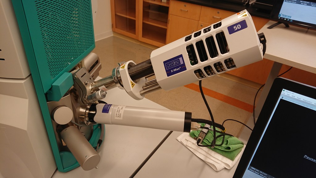
SEM
TESCAN VEGA3 LMU scanning electron microscope with LaB6 (or W) cathode that can be operated in a high-vacuum mode for coated/conductive specimens, as well as a low-vacuum mode for non-conductive specimens in their natural state.
Automated stage, secondary electron (SE) and backscatter (BSE) detectors.
Attachments
Nordlys Max 3 EBSD camera and XMaxN 50 EDS detector with Aztec Software.
Separate or simultaneous EBSD and EDS mapping, EDS point analyses.
EBSD
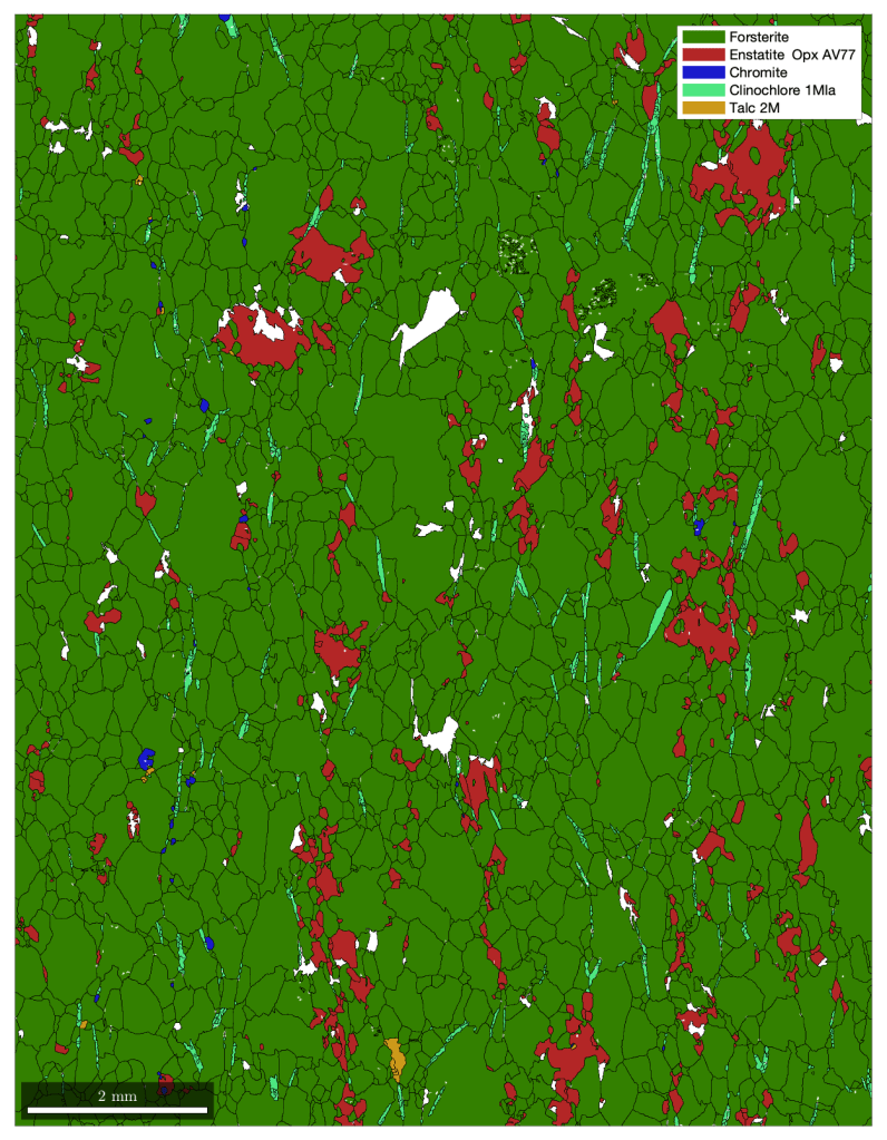


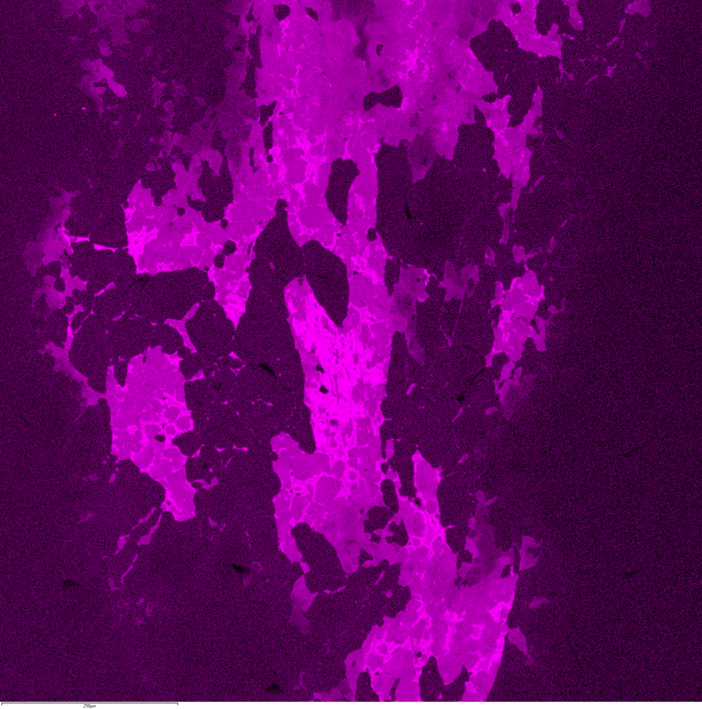
Phase map of a sample of Aheim dunite after processing of the raw data with MTEX. White areas are not indexed.
EBSD data color-coded by inverse pole figure. The similar colors of the majority of grains indicates a strong lattice preferred orientation.
Individual grains color-coded relative to the deviation from their mean orientation accentuating grain internal deformation. Gray colors indicate uniform orientation.
SE imaging

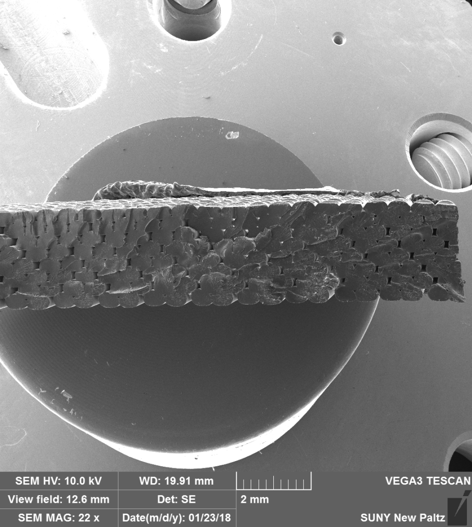
Fracture surface of 3-D printed plastic.
Example of a wide-field image. This enables easy navigation on large samples.

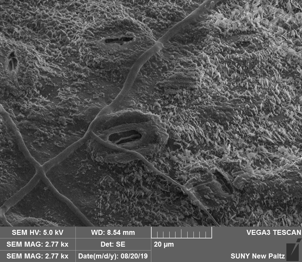
Stomata on a freshly picked oak leaf. Images were taken under high vacuum with sample as is.
Analysis
EDS map showing the distribution of Ca in a sample of Anita Bay peridotite. Brightest areas are melt and cpx, darker grains are Ca-rich opx. Olivine is darkest. Field of view: 1 mm
BSE imaging

BSE ‘panorama’ of a peridotite, optimized for contrast. Each image tile in the panorama is 1 mm on a side. Dark grains are orthopyroxene, lighter gray olivine.
Hourly Rates
Academic: $50
Commercial: $200
Contact
Address


Publications
- The effect of cooling during deformation on recrystallized grain-size piezometry, H. Soleymani, S. Kidder, G. Hirth and G. Garapić, Geology, 48, 531–535, 2020 (https://doi.org/10.1130/G46972.1), 2020.
- Generalized models for unidirectional anisotropic properties of 3D printed polymers, J. W. Nelson, D. Atkins, M. L. Gottstine, J. Yang, G. Garapić, S. Jaminion, A. Nelson, and K. Wilson, Rapid Prototyping Journal, (https://doi.org/10.1108/RPJ-03-2019-0083), 2020.
- Constraints on oxygen fugacity within metal capsules, U.H. Faul, C.J. Cline II, A. Berry, I. Jackson, G. Garapić, Physics and Chemistry of Minerals, (https://doi.org/10.1007/s00269-017-0937-7), 2018.
